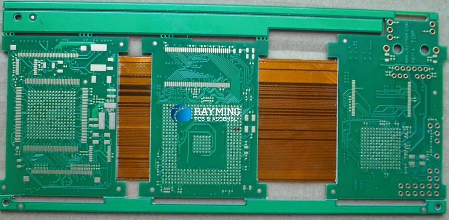
Rigid-flex PCBs contain both rigid PCB regions and flexible circuit sections enabling integration of interconnects that flex dynamically. This helps create electronics that can withstand vibration, motion or conform precisely to product form factors.
This article provides a step-by-step guide on designing and laying out rigid-flex boards using Altium to harness their benefits in integrated electronics projects. Core design rules, constraints, modeling and manufacturing outputs are covered.
Rigid-Flex PCB Overview

Combining multiple electronics sub-systems onto rigid-flex PCB structures brings reliability, space and weight savings over traditional wiring harnesses and connectors between separate boards. Lower part counts also reduce assembly costs.
Enabling technology developments include reliable flexible dielectric materials and high throughput machining to fabricate complex board shapes.
Design Stages and Planning

Successful rigid-flex PCB implementation requires both upfront planning and design considerations during layout and documentation phases:
Scope Stage
- Determine ideal partitioning between rigid and flex areas
- Select suitable flexible substrate materials
- Consult assembly team on process impacts
Design Stage
- Model distinct rigid and flex areas
- Apply specific rules and constraints
- Add reinforcement structures
- Document stackup and fabrication details
Careful planning focusing on manufacturability and assembly integration ensures reliable end products can be achieved.
Creating Rigid-Flex Regions
The first step is identifying constituent rigid and flexible areas of the design within Altium:
Rigid Regions
Standard fiberglass/epoxy FR4 PCB can define the rigid sections containing high component densities or interface connectors. Minimum length/width help withstand handling stresses.
Flex Areas
Flex material such as polyimide or PTFE/ceramic defines sections where dynamic contouring, vibration resistance and conformity are required. These span between rigid zones.
Split Planes
Classify where material transitions from rigid to flex. Minimum curvature rules guide placement to avoid failures initiating at corners.
With regions established, appropriate technologies can next be applied.
Rigid PCB Best Practices
Proven PCB layout techniques should first be applied within the rigid board sections:
- Define required layer stackup and materials
- Assign plane layers for power and signals
- Apply component footprints and circuitry
- Route signals with impedance control
- Include testpoints, fiducials, etc
Rigid areas typically contain most components, connectors and complex routing.
Flex PCB Best Practices
Specific considerations apply uniquely when laying out flexible areas:
- Model chosen dielectric material stackup
- Minimize feature sizes for reliability and resilience
- Eliminate rigid right angles setting bend radius rules
- Ensure castellations allow flex to exit rigid sections
- Include reinforcing structures to avoid dynamic tears/cracks
Following dedicated flexible PCB guidelines prevents common failure modes.
[Table summarizing PCB technology choices within Rigid-Flex designs]

Transitions and Reliability Rules
Handling the interface between rigid and flexible materials requires special modeling and rules to ensure reliability:
Split Planes
Define where material stackups change. Sharp corners concentrate damaging forces so curvature rules guide placement.
Castellated Edges
Alter coverlay/solder-mask layers to expose pads allowing cleanly exit of flex layers minimizing separation and cracking risk.
Corner Reinforcement
Additional adhesive plus barred features on corner pads creates smooth reliable transitions reducing crack initiation points.
Applying these techniques appropriately dissipates otherwise damaging mechanical stresses from vibration, shock and motion ensuring durability.
Documentation Outputs
Clear documentation communicating fabrication requirements, associated assembly implications and assisting testing procedures is key for first-time rigid-flex projects to succeed smoothly:
Layer Stack Legend
Define materials, copper weights and dimensions for all sections of the PCB including prepreg/adhesive bonding layers. Specify fabrication details like lamination process/pressure profiles. Provide electrical test acceptance criteria.
Assembly Drawings
Guide assembly staff through application-specific component population sequences including orientation, maximum device density and heating recommendations to activate bonding adhesives if needed. Supply test procedures.
Fabrication Drawings
Overlay mechanical outlines showing board contour dimensions, indicated cut-outs, material extents and coverlay termination points to assist fabrication programming and quality checks.
So while the PCB layout adapts familiar rigid and flexible design techniques in each region, comprehensive documentation detailing the integration for production is critical.
Conclusion
Rigid-flex PCB technology enables integration of dynamic flexible interconnects linking rigid board systems reliably. By appropriately planning and partitioning constituent sections then applying specialized rules guiding material transitions, engineers can harness benefits like reduced wiring, improved dynamic performance and compact form factors through Altium rigid-flex design and layout.
Clear documentation delivers vital supplementary information to smooth the path through fabrication and assembly turning conceptual models into successful functioning prototypes. As electronics aim for tighter integration in challenging environments, rigid-flex represents an enabling design platform warranting consideration.
Frequently Asked Questions
How are components assembled on flex regions of rigid-flex boards?
As rigid substrates are preferable under components for stability and reduced stress, discrete devices are rarely mounted directly onto narrow flexible areas unless using compatible conductive flex adhesives. So techniques like cut-outs, pick-and-place brackets or manual glueing adapt traditional assembly.
What limits the minimum width of flex interconnect areas between rigid sections?
Excessively narrow neck regions magnify harmful dynamic peeling forces during flexing motion risking substrate or copper trace cracking after repeated bending cycles. Typically 4mm width is a minimum with 8mm or above preferred for robustness and assembly ease depending on thickness.
Why is impedance control difficult on flex PCBs?
Varying dielectric thickness when flexing together with limited shielding mean maintaining a target impedance through dynamic envelopes challenges even advanced fabrication. So matched lengths plus differential signals or modulation techniques provide reliable high speed transmission if needed.
How many bend cycles do flexible materials typically support?
Assuming quality fabrication and sufficient width at crossover points, flex laminates last 500 cycles minimum. With reinforcement such as bars 2,000+ cycles is readily achievable. Micro-cracks then precede complete failures beyond 5–10k full reversals. Suitable design margins mitigate wear-out risks.
Can conventional PCB repair techniques be used on rigid-flex boards?
Yes but with limitations. Rigid areas allow standard rework of components or conductors but flex zones prevent soldering or abrasion. Instead conductive epoxies, laser deletion or physical patches manually apply when repairs are essential. Lower temperatures and specialist tools are required throughout to avoid collateral damage across flex areas.


No comments:
Post a Comment