Sunday, January 28, 2024

How to Create PCB Fabrication and Assembly Drawings in Altium Designer

 Printed circuit boards (PCBs) form the backbone of electronic devices and products. Designing PCBs requires attention to detail in order to produce a functional, high-quality board that meets fabrication and assembly requirements. A key part of the PCB design process is generating clear, accurate fabrication and assembly drawings that communicate all necessary information to PCB manufacturers.

Altium Designer is a leading PCB design software that enables designers to take ideas from concept through to fabrication and assembly. This comprehensive software includes robust tools for producing all needed PCB drawings.

This guide will walk through the complete process for creating professional PCB fabrication and assembly drawings in Altium Designer, including:

  • Setting up output job files
  • Generating fabrication drawings
  • Mechanical layers
  • Drill drawings
  • Panelization drawings
  • Creating assembly drawings
  • Assembly drawings
  • Pick and Place files
  • BOM/Component information
  • Final file outputs

Follow these steps to smoothly guide your PCB project from prototype through volume production.

Setting Up Output Job Files

The first step is to set up Output Job files within Altium to prepare for generating all your needed fabrication and assembly drawings. Output jobs allow you to easily configure and generate sets of outputs with just a few clicks.

Create New Output Jobs

Under the Project menu, select Add New to Project > Output Job. This will open the Add New to Project window — select Output Job then click OK.

This adds an empty Output Job file to the project. Double click on the new .OutJob file to open the OutJob editor.

In the Properties panel on the right side, name your Output Job file based on its purpose, such as “Fabrication” or “Assembly.”

Configure Output Containers

Within the OutJob editor, containers are used to configure sets of related outputs. Containers allow you organize all the drawings, files, documentation, and other data needed to manufacture your boards.

Under Outputs in the editor, right click and select Add New Output Container. Name the first container Fabrication and set the following properties:

  • Description: Drawings and data needed for PCB fabrication
  • Target Output Directory: Set to project folder/Fab (for example)

Follow the same steps to create a second container named Assembly for assembly drawings and documentation.

These containers will group all related fabrication and assembly files generated from the Output Job.

Add Output Generators

With output containers set up, the next step is to add output generators — these generators will produce the needed drawings, plans, and files related to fabrication and assembly.

Under each container, right click and select Add New Output to add generators. For the Fabrication container, add generators for:

  • Fabrication Drawings
  • Drill Drawing/Report
  • Panel Drawing

For the Assembly container, add generators for:

  • Assembly Drawings
  • Pick Place Files
  • Bill of Materials

For each generator, check the properties panel to configure settings as needed. For now, the default settings are fine.

Creating Fabrication Drawings

The configured Output Job will now generate all fabrication and assembly drawings and files needed to manufacture the PCB based on generators added. First we will walk through fabrication drawings.

Generate Mechanical Layers

Mechanical layers communicate key details on physical board characteristics needed for fabrication. This includes layer colors, materials, finishes, thickness, and more.

To output mechanical layer drawings:

  1. Under Fabrication container, select the Fabrication Drawings generator
  2. Set the Layers field to Mechanical Layers
  3. Check that PDF format is selected
  4. Click on the Run button

This will take the currently open PCB document and output a PDF drawing with all mechanical layer information. The PDF will be created in the Fab output folder.

Review the layers and details in the generated mechanical drawing PDF to ensure accuracy.

Create Drill Drawings
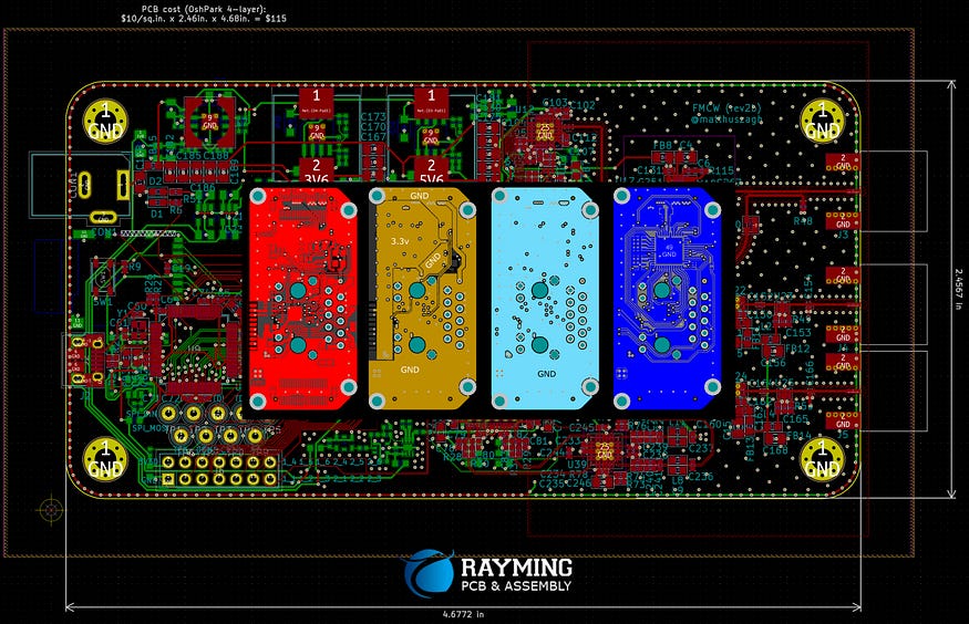
Drill drawings provide PCB drill information showing hole sizes and locations. Separate drawings are needed for plated and non-plated holes.

To create drill drawings:

  1. Under Fabrication container, select the Drill Drawing/Report generator
  2. Check Print drawing frame option
  3. Set Drill Drawing Type to Plated
  4. Click Run to generate plated holes drawing
  5. Repeat steps changing Drill Drawing Type to NonPlated to generate non-plated holes

This outputs PDF drawings showing plated and non-plated drill locations and sizes need to precisely drill the PCB.

Generate Panelization Drawings

Panelization drawings are used to lay out PCBs efficiently on panel sheets for volume production. These drawings optimize space usage across panels.

To create panelization drawings:

  1. Under Fabrication container, select the Panel Drawing generator
  2. Check Print frame on all output formats
  3. Click Run to output panel drawing PDF

Review the panel drawing to ensure proper alignment and spacing between panels and boards.

This covers key fabrication drawing requirements. Next we’ll look at generating assembly deliverables.

Creating Assembly Drawings

Well-documented assembly drawings and data enables smooth manufacturing and improves quality for assemblers. This includes assembly drawings, pick-and-place files, BOMs, and other specifics.

Generate Assembly Drawings

Assembly drawings illustrate how components are placed on the board from both top and bottom sides. This aids assemblers for high quality component population.

To output assembly drawings:

  1. Under Assembly container, select the Assembly Drawings generator
  2. Check boxes for Board OutlineMechanical LayersTop Overlay, and Bottom Overlay layers
  3. Click Run

The resulting PDF contains clear views of top and bottom layers indicating precise component placements.

Output Pick and Place Files

Pick-and-place files provide assemblers with x/y location coordinates for automated component placement machinery.

To export pick-and-place info:

  1. Under Assembly container, select the Pick Place File generator
  2. Ensure file type is CSV
  3. Click Run

The output pick-and-place CSV file contains key fields for assembly machines including Designator, Comment, Mid X, Mid Y, Ref X, Ref Y, and Rotation.

Export Bill of Materials

An up-to-date bill of materials (BOM) listing all components is critical to manage procuring and kitting parts for assembly.

To output BOM data:

  1. Under Assembly container, select Bill of Materials generator
  2. Set output format to CSV
  3. Enable all columns in BOM Settings
  4. Click Run

This exports complete BOM data into a CSV — including Designators, Description, Part Numbers, Quantities, Manufacturers, and Extensive Parameters.

Final Outputs

Once all output generators are configured, generating a full set of fabrication and assembly files is easy:

  1. Select the top-level Output Job in the project pane
  2. Click Generate Outputs or press F6
  3. Browse generated folders to access all PDF drawings, CSV data, and other output documents

This single action will produce complete documentation needed by your PCB manufacturer and assemblers for prototyping through volume production.

Be sure to review all drawings for completeness and accuracy. Rerun generators if any changes are made to the board. Keep output folders up to date as the design iterates.

Conclusion

Altium Designer’s robust output generation capabilities helps designers seamlessly create detailed PCB fabrication and assembly documentation critical for manufacturing. Configuring Output Jobs streamlines exporting all necessary drawings and data needed for production.

With a properly configured Output Job file, high quality documentation to support PCB fabrication, testing, assembly, procurement, and other manufacturing functions is just a click away. Keeping output documentation synchronized with any design changes ensures smooth transition from prototype through volume manufacturing.

Frequently Asked Questions

What are the key fabrication drawing requirements?

The most important fabrication drawings include:

  • Mechanical layers showing board materials, finishes, thickness, colors
  • Drill drawings detailing hole sizes and placements
  • Panelization drawings arranging multiple PCBs on panel sheets

What assembly documentation is critical for PCB assemblers?

Vital assembly documentation includes:

  • Assembly drawings illustrating component placement from top and bottom
  • Pick-and-place files with x/y machine locations
  • Bill of

Saturday, January 27, 2024

How to Implement a Watchdog Timer in Your PCB Design

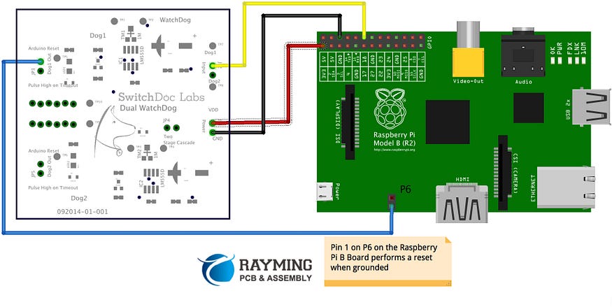
 Watchdog timers (WDT) are circuits that trigger automatic system resets to recover from unexpected software or hardware faults in embedded electronics preventing system lockup or freeze.

This article provides a step-by-step guide on how to implement a fail-safe timer in PCB designs using dedicated microcontroller modules or discrete logic. Circuits to connect and configure external components are covered to safely automate resets ensuring reliable operations.

WDT Operating Principles

A watchdog timer is configured to periodically trigger electrical pulses at pre-determined intervals unless continuously reset by the primary software/firmware flow beforehand. If the main controller program flow stalls or crashes preventing the periodic reset of the WDT, it will eventually overflow activating the timer’s output pin.

This pin can be connected to the external or integrated hardware reset input present on most microcontrollers that forces a full system restart returning operation to a known good software initialization state after any unforeseen fault event.

[Figure showing basic operating principle of a watchdog timer module]

Key advantages over manual resets include:

  • Swift automated recovery independent of stalled code flow
  • No external intervention needed enabling deployment in remote equipment
  • Option to enter fail safe modes or safe states upon watchdog fault before restart

So WDT technology delivers self-correcting resilience.

Microcontroller Integrated WDT Modules

Many modern microcontroller units integrate one or more watchdog timer modules internally that equip systems with built-in recovery capabilities:

Dedicated Module — Self-contained timer block is clocked independently allowing configuration of timeout period from milliseconds up to minutes matched against system reset requirements.

Triggers Reset — Specialized WDT recovery pin connects internally to the MCU reset circuit automatically. So on overflow, the module directly forces entire chip restart without external intervention.

Minimal Components — Integrated configuration registers allow enable/disable, timing adjustment, trigger action setup eliminating most external discretes otherwise needed.

Software Integration — WDT kick function written into main program code flow resets module periodically to continually avert timeout ensuring SW health.

So internal units provide reliable and convenient system protection at marginal cost.

External Watchdog ICs

For processors lacking sufficient internal watchdog provisions or where independent external monitoring is preferred, dedicated timer management ICs can be deployed:

Package Options — Choose among SOT23–5, SOIC-8 or TSSOP-14 packages depending on features/space needs with supply voltages from 1.8V to 5.5V. Larger particles offer multiple channels.

Configurability — Adjustable or fixed time-out periods with up to minutes range together with manual or electrical trigger modes cater to different reliability objectives.

Monitoring — Separate supply and clock domains with fault notification outputs ensure robust oversight should primary Domain risks materialize. Heartbeat check-ins between host MCU and Watchdog IC provide health indication.

System Interface — Simple digital logic integration oversees MCU activity resetting countdown on periodic receipt of alive pulses or else forcing dedicated reset pin activation after delays expire reviving unresponsive processors.

So discrete WDT ICs bolster resilience even on processors lacking native safety provisions.

Implementation Factors

Successfully deploying either internal or external watchdogs relies on four main factors during PCB implementation:

Trigger Timing — Set expiration periods allowing for maximum expected software latency margins. Too short risks premature needless resets while overlong delays system recovery losing data.

Clock Independence — Separate watchdog clock domains prevent stalled system clocks impacting supervision. A dedicated oscillator or RTC source works for External ICs while internal WDT modules leverage proprietary fail-safe clocking.

Reliable Reset — Low impedance paths to reset pins must assert signals positively. Verify reset duration meets microcontroller requirements for complete reboot.

Software Integration — Final factor is configuring kick instructions at optimal checkpoints in application software flows to continually refresh watchdog well within trigger periods to preempt unwarranted system recovery events.

Carefully applying these considerations ensures watchdogs deliver robust resilience improvements for mission-critical applications.

External Kick Circuits

Some scenarios demand forcing watchdog test kicks externally to validate reset paths or simulate fault injection assisting longer term reliability testing:

Manual Inputs — Connect push buttons to timer inhibition inputs allowing manual timer reset kicks at convenient intervals to avoid automated timeout trips verifying reset connectivity.

Test Controller — For rigorous reliability validation regimes, connect automated test sequencers to force variable duration watchdog deactivation sequences proactively introducing fault exposures while monitoring system recovery metrics gathering qualification data.

Voltage Checks — Analog voltage supervisors also link externally confirming operating thresholds remain within nominal window ranges otherwise initiating kicks to prevent noisy irregular supplies inadvertently disrupting microcontroller programming flows before resetting clocks.

So properly designed interfaces help strategically exercise watchdog test modes.

Layout Considerations

PCB physical layout also influences watchdog effectiveness especially avoiding faults that themselves obstruct resets during crashes:

Supply Microcuts — WDT modules need clean regulated voltage requiring thorough de-coupling placements and uninterrupted low impedance connections to generator sources using multiple vias/stitching traces on inner layers.

EMI Shielding — Guard voltage and timing/control signal paths against electromagnetic interference which may distort critical kick pulses or trigger thresholds especially on exposed outer layers.

Signal Integrity — Avoid impedance discontinuities on reset lines that reflect waveforms reducing integrity. Carefully match trace widths to target far-end impedance driving reset pin maximizing edge sharpness.

Test Points — Include voltage and logic test pads discretely branched allowing safe monitoring of supervisor inputs plus MCU reset acknowledgements through bring up validating full oversight signal chains.

So purposeful PCB layout precautions reinforce robust WDT functionality shielding external threats that themselves jeopardize fail-safe protections.

Conclusion

Implementing hardware watchdogs either via dedicated internal timer modules integrated on advanced microcontrollers or deploying standalone watchdog supervision ICs forms a key pillar for enhancing system reliability against unexpected faults.

Their automated reset signaling prevents indefinite lockup allowing swift recovery complementing software domain techniques like exception handling and redundancy. When thoughtfully configured matching reliable reset assertions with optimal trigger periods synchronized against application flow kick instructions, watchdog timers deliver vital fail-safe protections for mission critical embedded PCB designs.

Frequently Asked Questions

How do I determine the ideal watchdog timeout period?

Factors including the application’s maximum interrupt latency, boot time and clock tolerance help guide ideal timeout values preventing false or premature timeouts allowing successful kicks while still quickly detecting genuine stalls. Margin above software jitter provides buffer room.

Can the same watchdog supervise multiple microcontrollers?

Yes, some watchdog ICs provide multiple timer channels each with independent configurations monitoring several target systems simultaneously. So a single WDT device could oversee a trio of processors granting modular scalability.

Is it better to use an internal or external watchdog module?

External watchdogs provide independent oversight should primary controller resources themselves fail. But built-in WDT modules minimize component count/cost while simplifying software integration and avoiding signal routing needing greater isolation. Hybrid pairings harness both techniques for defense-in-depth.

How do I test my PCB’s watchdog response ahead of deployment?

Strategic test points discretely tapping watchdog kick pulses and system reset signals paired with purposeful omission or insertion of timer refresh kick instructions allows simulating crashes to validate end-to-end system restarts verifying watchdog effectiveness ahead of production.

Can I run independent watchdogs on separate voltages domains?

Yes, multi-supply systems can feature watchdog modules on alternate power rails overseeing respective domains. This grants compartmentalized protection with dedicated reset signaling per voltage allowing isolated recovery should specific generators exhibit issues.

AutoCAD-DXF Import-Export Support in Altium Designer You Should Know

 During electronics design projects, integrating PCB layout closely with mechanical enclosures and Module housings defined in MCAD tools requires exchange of precise 2D/3D models. AutoCAD’s DXF format bridges this interdisciplinary gap.

This article examines built-in AutoCAD-DXF file support within Altium Designer to smooth multi-tool workflows improving design quality through cross-domain collaboration while increasing engineering productivity.


AutoCAD-DXF Formats Overview

Autodesk’s AutoCAD software utilizes the .DXF file format for importing/exporting vector images between 2D drafting, mechanical modeling and PCB design tool environments:

DXF 2D — Vector line/arc contours defining mechanical enclosure outlines, holes, screw bosses, internal shelf profiles and clearance envelopes with precise dimensions.

DXF 3D — 3D shapes and extruded surface models visualizing end-product enclosures with mounted PCBs for spatial validation.

These portable digital definitions drive fabrication, integrate mechanical fit checks and validate product assembly intent.

Typical Multi-Tool Design Scenarios

Current trends see integrated electronics products spanning electrical and mechanical engineering disciplines adopting MCAD-ECAD tool chains:

Complex Enclosures — Multi-PCB systems in rugged, thermally demanding mechanically intricate housings require close 3D collaboration between electrical and mechanical teams from early design stages.

Component Clearances — Tight spacing of height-restricted internal sub-assemblies like radio modules or connectors often needs mechanical coordination to interface PCB layouts with housing spatial provisions through iterative adjustment until trade-offs balance.

Additive Manufacturing — New design-for-manufacturing (DFM) approaches around metal 3D printing, molding and casting introduce mechanical considerations directly from the start influencing component placement layout decisions based on optimal printed part strength, surface finish and assembly access directions.

[Figure showing example rugged electronics enclosure requiring ECAD-MCAD tool integration]

These emerging scenarios make smooth data exchange between AutoCAD and Altium vital for new product development success.

DXF Export from Altium

Generating 2D-DXF profiles containing accurately dimensioned board outlines, hole patterns, component clearance zones and placement locations enables mechanical fitment design in AutoCAD tools:

Setup — Define DXF output folder destination, specify desired layers for export inclusion and determine level of graphics/text detail.

Generate Output File — Trigger 2D drawing sheet export with or without dimensions as a multi-layer DXF containing planes, pads, holes, silk screen artwork, board profiles, text markings and origin/alignment fiducials.

Open in AutoCAD — AutoCAD tools then interpret imported .DXF files with various embedded PCB profiles and cut-outs assisting placement decisions and enclosure wall clearances around specific regions if needed.

So DXF exporting provisioning provides vital PCB zone data enabling mechanical housing design alignment.

DXF Import to Altium

Export from AutoCAD — Define target PCB zones as 2D/3D .DXF models containing mechanical envelopes with screw bosses, stand-offs, spatial allocations per module, wall thicknesses and connector placements relative to external housing form factor.

Setup in Altium — Determine mapping configuration for interpreting specific DWG/DXF layers into equivalent PCB documents or components. Set scaling precision between tools if dimensions differ.

Import .DXF Data — This assimilates AutoCAD models placing boundary limitations, spatial reservations and fixed mechanicals onto PCB canvas allowing engineers to visually arrange board layouts taking into account mechanical constraints right from conceptual stages.

So AutoCAD-native data flows into Altium workflows improving multi-domain new product introduction coordination.

[Table summarizing typical MCAD-ECAD exchange use cases employing DXF files]

ScenarioExchange PurposeComplex EnclosureVisual fit check, cooling, service accessInternal ClearancesValidate height budget allocationsAdditive ManufacturingOptimize orientations and reduce artifacts

Advanced Bidirectional DXF Manipulation

For advanced projects with continually evolving design constraints across tools, repetitive bidirectional DXF export and import between Altium and AutoCAD combines to enable interactive options:

Parametric PCB Models — By linking native DXF footprint models to software parameters, housing wall thicknesses or screw boss heights can adapt in tandem with ECAD component rearrangements through scripted behaviors as PCB layouts alter.

Semi-Automatic Reimporting — Configuring smart folder data monitoring paired with custom file handlers can automatically re-import updated DXF files from linked network locations enabling background assimilation of mechanical changes rather than manual imports.

Evolutionary Optimization — Adaptive layout tuning can incrementally shift component placements within electrical and thermal operating constrains while simultaneously judging housing model collisions until passing mechanical clearances across DXF tools.

So moving beyond simply static file exchange, dynamic DXF workflows actively support design evolution convergence between disciplines improving outcomes.

Unified Design Environment Strategies

Looking ahead, integrating ECAD tool electronics design refinement workflows directly inside full 3D MCAD environments Via unified interfaces aims to eliminate intermediary files through multi-domain collaboration visibility:

Associative Modeling — Rather than file exchange roundtrips, unified design environments directly associate electrical and mechanical model elements between tools keeping them perpetually synchronized as attributes alter.

Convergent Workspaces — Next generation tool ecosystem architectures allow disparate engineering teams to examine product designs across electrical and mechanical domains in shared virtual workspaces through messaging, notifications and secured access facilitating early collaboration.

Cloud-Hosted Data — Unifying design data on centralized cloud platforms accessed through web thin clients mitigates version control, facilitating real-time exchange avoiding delays shipping large local files between domain experts across global sites.

So while direct standards-based DXF import/export provides short term multi-tool integration today, converged unified design platforms represent the long term future for holistic new product introduction.

Conclusion

This article has explored how AutoCAD’s widely supported DXF 2D/3D file exchange bridge helps unify design intent between electrical and mechanical domains as products increase system complexity. Altium Designer’s built-in interoperability expediting roundtrip workflows through either simple clean data handoffs or active scripted synchronization assists engineering teams multifunctional tool environments.

As integrated electronics solutions become ever more sophisticated requiring tight coordination across electrical, industrial, workflow and interface design balancing aesthetics, performance and manufacturability goals, unified platforms will emerge facilitating visibility minimizing traditional engineering silos. Until then adaptable intermediate exchange formats like DXF provide productivity and quality gains.

Frequently Asked Questions

What are some pros and cons of intermediate file exchange vs unified tools?

Intermediary Files — Quick to implement but can drift without active sync. Formats can handle variety of tools. Lightweight integration.

Unified Tools — Eliminates synchronization issues but challenges integrating niche tools needing customization. Tightly couples update frequencies/testing.

When importing DXF housing models, what setting helps align layers?

Using layer mapping configuration enables directing source DXF elements into matching PCB layers by purpose to assimilate external housing data smoothly. Default settings can misalign otherwise.

How can I validate clearance tolerances post DXF import?

Performing clearance rule checks or collision queries on the PCB design after importing DXF enclosure models verifies electronics fit properly within allocated mechanical envelopes meeting target tolerances between housing and components.

What file format efficiently conveys PCB stackups and hole data?

Downloading a drill table or padstack file containing tool diameters paired with hole sizes efficiently shares multilayer stack planning details with external mechanical tools determining fastener engagement attributes aiding collaboration.

Can imported DXF models drive PCB component 3D step model placement?

Yes, integrating DXF housing data then linking PCB footprints to 3D step models allows placement of components visually confirming fit while checking housing lid clearance and assembly collision access seeing mounted internal electronics positioned ready for fabrication and mechanical integration given known design constraints.

Popular Post

Why customers prefer RayMing's PCB assembly service?

If you are looking for dedicated  PCB assembly  and prototyping services, consider the expertise and professionalism of high-end technician...