Saturday, January 27, 2024

How Does Altium Designer Help You Track Reference Designators on Your PCB

 Assigning clear reference designators to tracks, vias, components, nets and other features is vital for understanding PCB designs and correlating schematics to layout. Manually managing designators across complex boards with thousands of objects however introduces effort and risk of confusion.

This article examines how Altium Designer’s intelligent features automate and assist reference designator management across PCB projects. Techniques to track objects, synchronize schematic-layout changes and handle design evolution over time are covered to boost engineering efficiency and clarity.

Reference Designators Explained

A reference designator (RefDes) comprises alphanumeric IDs applied to PCB objects functioning as unique names that identify every individual item. RefDes take forms like:

  • R27 (Resistor #27)
  • C100 (Capacitor #100)
  • U3 (IC #3)
  • J4 (Connector #4)

Well-structured RefDes help identify components, nets, and tracks during design, assembly, test and field servicing. Serial numbering also conveys mounting sequence supporting automated production and providing order across complex systems comprising thousands of entities.

Manual Designator Assignment Challenges

Traditionally engineers manually assign reference designators to entities in both the schematic and PCB layout. Keeping these synchronized while evolving fluid designs introduces effort and risk of confusion across tools and engineers.

Altium Designer overcomes manual reference tracking with intelligent annotation and synchronization to boost engineers’ efficiency.

Automated Annotation and Synchronization

Altium Designer features specialized tools to automate annotation and synchronization workflows for designators between schematics and board layout files:

Schematic Annotation

assigns designators by annotating all required objects according to customizable naming rules applied consistently across entire projects. Engineers focus on connectivity rather than manually numbering thousands of devices.

Forward & Back Annotation

propagates any changes to designators between schematics and layout files automatically. This maintains consistency as designs evolve across tools preventing confusion and errors.

Layout Variants

enable specialized PCB version RefDes mappings to deal with sub-assembly modules, chassis zones, or manufacturing assembly sequences all while retaining schematic synchronization.

Together these features offload repetitive manual work to improve engineer productivity multifold.

[Table summarizing key automated annotation and synchronization capabilities]

Additional Helper Features

Besides core annotation and synchronization, Altium provides additional capabilities to track design changes related to reference designators:

Update on Modify

In the schematic editor, component renames directly carry across connected signals automatically rather than forcing manual edits across each linked net.

Highlight Net/Scheme

Visually traces entire net connectivity by highlighting when probing any pin or junction node. This visually validates circuit network continuity aiding debug.

Cross Probe

Clicking reference designators cross probes the item dynamically between schematic and PCB layout editors across tool boundaries to track objects.

Version Control Systems

Tie into software versioning tools like SVN or Git to track RefDes edits alongside broader project change management enabling reversion if needed.

Multiple features therefore assist keeping reference designators synchronized.

Design Variant Strategies

More advanced annotation techniques help manage complex projects seeing ongoing change across various hardware instantiations and platform integrations:

Incremental Flat Schemes

Here a simple naming convention adapts like U1_A, U1_B as incremental small modifications occur on a single baseline. This avoids renumbering unaffected sections.

Location/Zone Schemes

Partition complex boards into functional zones with localized independent naming schemes. This helps isolate and identify regions without disrupting other major sections tracking only local changes.

Family Naming

Define common root naming between associated modules/subsystems including generic descriptor suffixes denoting role alongside instance numbering. Ex: “ Controller01_A”. This scales to broader platform ecosystems and product families.

Applying these strategies future proofs reference designator tracking through projected design evolution embodiments based on scope.

Layout PCB Variants

A specialized Altium constructor enables discrete designator mapping files that translate annotation schemes between schematic and layout representations:

Variant .CMP file

Here the component mapping file works with layout variants to handle localized differences:

  • Sub-circuits split across chassis modules
  • Double sided assemblies with zone divisions
  • Manufacturing placement sequences

This adds great flexibility to adapt layout representations without disrupting logical schematics as the project evolves across deployable configurations.

Conclusion

In summary, rather than demanding engineers waste design time manually tracking reference designators as designs scale up, Altium Designer’s automated tools assign and synchronize annotations between schematics and board layouts. Additional helpers highlight nets and cross probe to boost understanding.

Extending core functionality, incremental and zonal designator schemes aided through variant mapping files future proof complex projects against ongoing changes across modules, chassis elements or product generations. Intelligent features therefore give engineers confidence in tracking every component reliably through designs comprising thousands of parts from concept to completion.

Frequently Asked Questions

How are reference designators handled for duplicate identical parts/values on a board?

Where duplicate components share the same value, automated schematic annotation appends index numbers to their core reference ID for uniqueness while retaining consistency.

For example resistor R27 may become R27_1, R27_2 etc. if multiple identical resistors are present. This avoids confusion while indicating quantities of each device value.

What naming elements can I include in custom defined annotation scheme rules?

Typical annotation scheme elements include:

  • Prefix — Component type (R, C, U)
  • Instance Index — Unique sequential number (1, 2, 3..)
  • Base Index — Shared root identifier
  • Location ID — Board region/zone
  • Suffix — Variant descriptor

Can changes be tracked between schematic revisions and board layout iterations?

Yes, layout snapshots can capture PCB states at the time of each schematic revision. Annotation differences highlight changes between design iterations for robust version control and component tracking.

How are reference designators handled in multi-channel schematics?

Multi-channel sheets may represent separate functions or circuit blocks while Altium annotation can either number sequentially across all sheets or partition numbering into localized zones through assignment rules. Global numbering toggles help switch modes.

If I change a component, why do the connected net names not update?

While Altium handles forward/back annotation of core reference designators between tools, by default it does not automatically rename associated net names. This avoids unintended widespread naming disruption. Simple manual synchronization retains clarity.
Friday, January 26, 2024

How to Design a Rigid-Flex PCB in Altium

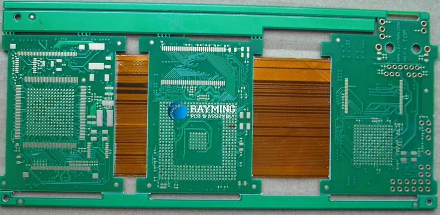
 Rigid-flex PCBs contain both rigid PCB regions and flexible circuit sections enabling integration of interconnects that flex dynamically. This helps create electronics that can withstand vibration, motion or conform precisely to product form factors.

This article provides a step-by-step guide on designing and laying out rigid-flex boards using Altium to harness their benefits in integrated electronics projects. Core design rules, constraints, modeling and manufacturing outputs are covered.

Rigid-Flex PCB Overview

Combining multiple electronics sub-systems onto rigid-flex PCB structures brings reliability, space and weight savings over traditional wiring harnesses and connectors between separate boards. Lower part counts also reduce assembly costs.

Enabling technology developments include reliable flexible dielectric materials and high throughput machining to fabricate complex board shapes.

Design Stages and Planning

Successful rigid-flex PCB implementation requires both upfront planning and design considerations during layout and documentation phases:

Scope Stage

  • Determine ideal partitioning between rigid and flex areas
  • Select suitable flexible substrate materials
  • Consult assembly team on process impacts

Design Stage

  • Model distinct rigid and flex areas
  • Apply specific rules and constraints
  • Add reinforcement structures
  • Document stackup and fabrication details

Careful planning focusing on manufacturability and assembly integration ensures reliable end products can be achieved.

Creating Rigid-Flex Regions

The first step is identifying constituent rigid and flexible areas of the design within Altium:

Rigid Regions

Standard fiberglass/epoxy FR4 PCB can define the rigid sections containing high component densities or interface connectors. Minimum length/width help withstand handling stresses.

Flex Areas

Flex material such as polyimide or PTFE/ceramic defines sections where dynamic contouring, vibration resistance and conformity are required. These span between rigid zones.

Split Planes

Classify where material transitions from rigid to flex. Minimum curvature rules guide placement to avoid failures initiating at corners.

With regions established, appropriate technologies can next be applied.

Rigid PCB Best Practices


Proven PCB layout techniques should first be applied within the rigid board sections:

  • Define required layer stackup and materials
  • Assign plane layers for power and signals
  • Apply component footprints and circuitry
  • Route signals with impedance control
  • Include testpoints, fiducials, etc

Rigid areas typically contain most components, connectors and complex routing.

Flex PCB Best Practices

Specific considerations apply uniquely when laying out flexible areas:

  • Model chosen dielectric material stackup
  • Minimize feature sizes for reliability and resilience
  • Eliminate rigid right angles setting bend radius rules
  • Ensure castellations allow flex to exit rigid sections
  • Include reinforcing structures to avoid dynamic tears/cracks

Following dedicated flexible PCB guidelines prevents common failure modes.

[Table summarizing PCB technology choices within Rigid-Flex designs]

Transitions and Reliability Rules

Handling the interface between rigid and flexible materials requires special modeling and rules to ensure reliability:

Split Planes

Define where material stackups change. Sharp corners concentrate damaging forces so curvature rules guide placement.

Castellated Edges

Alter coverlay/solder-mask layers to expose pads allowing cleanly exit of flex layers minimizing separation and cracking risk.

Corner Reinforcement

Additional adhesive plus barred features on corner pads creates smooth reliable transitions reducing crack initiation points.

Applying these techniques appropriately dissipates otherwise damaging mechanical stresses from vibration, shock and motion ensuring durability.

Documentation Outputs

Clear documentation communicating fabrication requirements, associated assembly implications and assisting testing procedures is key for first-time rigid-flex projects to succeed smoothly:

Layer Stack Legend

Define materials, copper weights and dimensions for all sections of the PCB including prepreg/adhesive bonding layers. Specify fabrication details like lamination process/pressure profiles. Provide electrical test acceptance criteria.

Assembly Drawings

Guide assembly staff through application-specific component population sequences including orientation, maximum device density and heating recommendations to activate bonding adhesives if needed. Supply test procedures.

Fabrication Drawings

Overlay mechanical outlines showing board contour dimensions, indicated cut-outs, material extents and coverlay termination points to assist fabrication programming and quality checks.

So while the PCB layout adapts familiar rigid and flexible design techniques in each region, comprehensive documentation detailing the integration for production is critical.

Conclusion

Rigid-flex PCB technology enables integration of dynamic flexible interconnects linking rigid board systems reliably. By appropriately planning and partitioning constituent sections then applying specialized rules guiding material transitions, engineers can harness benefits like reduced wiring, improved dynamic performance and compact form factors through Altium rigid-flex design and layout.

Clear documentation delivers vital supplementary information to smooth the path through fabrication and assembly turning conceptual models into successful functioning prototypes. As electronics aim for tighter integration in challenging environments, rigid-flex represents an enabling design platform warranting consideration.

Frequently Asked Questions

How are components assembled on flex regions of rigid-flex boards?

As rigid substrates are preferable under components for stability and reduced stress, discrete devices are rarely mounted directly onto narrow flexible areas unless using compatible conductive flex adhesives. So techniques like cut-outs, pick-and-place brackets or manual glueing adapt traditional assembly.

What limits the minimum width of flex interconnect areas between rigid sections?

Excessively narrow neck regions magnify harmful dynamic peeling forces during flexing motion risking substrate or copper trace cracking after repeated bending cycles. Typically 4mm width is a minimum with 8mm or above preferred for robustness and assembly ease depending on thickness.

Why is impedance control difficult on flex PCBs?

Varying dielectric thickness when flexing together with limited shielding mean maintaining a target impedance through dynamic envelopes challenges even advanced fabrication. So matched lengths plus differential signals or modulation techniques provide reliable high speed transmission if needed.

How many bend cycles do flexible materials typically support?

Assuming quality fabrication and sufficient width at crossover points, flex laminates last 500 cycles minimum. With reinforcement such as bars 2,000+ cycles is readily achievable. Micro-cracks then precede complete failures beyond 5–10k full reversals. Suitable design margins mitigate wear-out risks.

Can conventional PCB repair techniques be used on rigid-flex boards?

Yes but with limitations. Rigid areas allow standard rework of components or conductors but flex zones prevent soldering or abrasion. Instead conductive epoxies, laser deletion or physical patches manually apply when repairs are essential. Lower temperatures and specialist tools are required throughout to avoid collateral damage across flex areas.

Are Fiducial Marker Placements on PCBs Still Necessary with The Lastest Manufacturing Capabilities?

 Fiducial markers have been relied upon in printed circuit board (PCB) design and manufacturing for decades to accurately align layers and facilitate reliable automated assembly. However with continual advances in fabrication and assembly equipment, are these alignment markers still a necessary part of modern PCB design?

This article examines the role fiducials serve across the PCB production workflow while assessing alternatives to determine if their inclusion on designs remains justified given the capabilities of current manufacturing processes. Core alignment techniques are compared and key factors influencing fiducial requirements are explored.

Fiducial Marker Overview

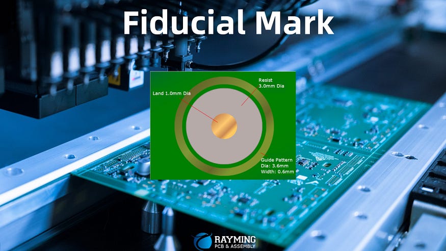
Fiducials are printed circular pads, often comprised of copper located in unused board areas outside the component footprint regions and circuitry. They serve as visual reference markers for camera-aided alignment and registration.

[Figure of typical fiducial markers on a PCB design file]

Fiducials assist equipment to dynamically orient, scale and account for distortions within the manufacturing process. This improves alignment accuracy between layers during fabrication in addition to component placement precision.

Role Across the PCB Production Workflow

To understand whether fiducials are still relevant, it is worth examining where they are utilized in the production process:

Fabrication

During PCB fabrication, fiducials facilitate layer-to-layer registration and alignment. Optical inspection compares fiducial locations between each layer to detect and correct layer misalignments before lamination.

Assembly

Later, during automated assembly, pick and place machines again rely on fiducials to determine the exact orientation and scale of PCBs. Component placement positions can then be adapted to improve accuracy.

Test and Inspection

Finally, automatic optical inspection (AOI) equipment utilizes fiducials to align boards and testing probes ensuring repeatability between fab runs.

Layer Alignment Alternatives

Modern PCB fabrication utilizes alternative techniques to align layers that potentially reduce or eliminate reliance on fiducials. The efficacy of these methods determines ongoing fiducial necessity.

Mechanical Pin Registration

Similar to traditional photographic film techniques, layer stacks can be aligned using precision pins that mate with cut-outs in the panelized board material during lamination when the layers are fused together into the final board.

By ensuring global mechanical alignment persistently through the entire stackup with pins that penetrate through multiple layers, this technique does not require intermediate fiducials.

However mechanical registration has limitations on complex, high mix boards. Achieving tolerances below 100μm (±.004”) also becomes challenging at volume production scale across large panelized boards.

Laser Direct Imaging (LDI)

LDI photoplotters utilize optical scaling techniques to dynamically map distortions by scanning registration markings on individual layers and computing compensation factors. This facilitates alignment as each layer artwork is directly ablated onto raw copper foil prior to lamination through a single equipment setup.

Being applied at the individual layer level circumvents extensive laminate shrinkage and distortion accumulating across a multilayer stackup. Layer misalignment below 25μm (±.001”) is consistently achievable.

Laser scaling still requires some registration markings but their count can be minimized if supplemented with tighter process controls that reduce distortions occurring throughout fabrication.

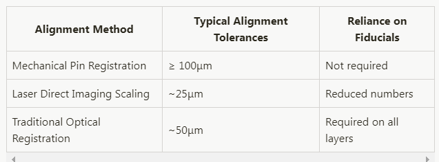
[Table comparing traditional fiducial dependent registration against modern alternatives for fabrication alignment]

Alignment MethodTypical Alignment TolerancesReliance on FiducialsMechanical Pin Registration≥ 100μmNot requiredLaser Direct Imaging Scaling~25μmReduced numbersTraditional Optical Registration~50μmRequired on all layers

Assembly Alternatives

Emerging assembly technologies provide fiducial-less component placement alternatives potentially reducing reliance on PCB fiducials for this application also.

On-Machine Optical Verification

Advanced pick-and-place machines integrate higher resolution cameras together with optical inspection that measures warp and calculates scaling factors dynamically for each board.

This closed-loop system adapts component placement in real-time to detected PCB distortions eliminating reliance on static fiducial locations. Mapping the entire board surface improves tolerance across full board areas rather than only at discrete fiducial points.

Component Embedding/X-Ray Registration

Another technique gaining adoption is embedding radio-opaque reference markers into plastic packaged-components such as QFN/QFPs. X-ray imaging then detects these markers placing components precisely irrespective of PCB distortion.

This embedded reference system ensures perfect registration between components and board features since they move in unison avoiding many common placement defects.

When Fiducials Are Still Necessary

While modern fabrication and assembly technologies provide alternative alignment strategies in many situations, certain applications still rely heavily on board-level fiducials.

High Density Interconnect (HDI)

With line width/spacing below 4 mil, fiducial visual references facilitate tight optical overlay registration control through fabrication. Mechanical registration limitations preclude its use for microvia HDI layer alignment.

High Mix, Quick Turn Prototyping

Where maximizing fabrication flexibility and minimizing changeover is prioritized, use of mechanical pin registration is often impractical whereas optical fiducial scaling supports high mix requirements.

Fine Pitch Components

As component pin-pitch continues shrinking below 0.4mm requiring placement tolerance below 50μm, on-machine vision systems struggle without fiducial assistance to detect pad/lead distortions at these minute scales.

Large Board Sizes

Larger PCB sizes exacerbate the challenge of minimizing and compensating distortions making some quantity of fiducials still beneficial for scaling alignment across full board areas.

Double-Sided SMT Assemblies

Fiducials assist optical alignment between both sides of double-sided SMT assemblies where components exist on opposite sides of the PCB that must align precisely.

So while technological advances may transform fiducial requirements in many PCB production scenarios, they remain beneficial in certain applications.

Conclusion

In summary, innovations in fabrication laser imaging and assembly equipment vision precision reduce reliance on traditional PCB fiducials for layer alignment and component placement in typical situations. Completely eliminating them however reduces flexibility currently still necessary to support specialized HDI, large panel or fine pitch technology boards.

As manufacturing capabilities further improve and alternative techniques mature to displace optical fiducial registration, minimal counts rather than complete removal may strike the right balance for most applications still maintaining contingency processing backup. When specifications demand the highest precision at significant volumes, embedded references in packaging or auxiliary sub-assembly stages appear the ultimate path to displace direct board fiducials longer term.

Frequently Asked Questions

What are some key alignment tolerance benchmarks between fabrication and assembly processes?

  • PCB Fabrication layer alignment: ≤ 25μm
  • PCB Assembly component placement: ≤ 50μm
  • High density (HDI) fabrication: ≤ 10μm

What proportion of surface area do fiducials typically occupy on a given design?

As few as four fiducials occupying less than 0.01% of total board space is common. Even designs with higher fiducial counts target allocation below 0.05% allowing components and circuitry to utilize the vast majority of available PCB surface area.

How do costs of alignment accuracy compare between fiducials, mechanical pinning and embedded package references?

Mechanical pin registration has a higher initial cost but saves on inspection. Embedded references must be applied to all components whereas fiducials have negligible impact individually being PCB-only features. Overall across entire volumes, advanced methods can provide total cost savings through yield and quality improvements.

How have tolerances changed as PCB technology scaled up panel sizes and scaled down features?

Panel sizes now exceeding 600 x 600 mm are 100x greater area than early PCB fabrication. Conversely line width/spacing has reduced below 25μm which is nearly 10x finer than predecessors. These trends demand alignment methods that excel at both macro and micro precision scales simultaneously.

Why do technicians still manually align layers and perform optical inspection in fabrication facilities?

While processes are highly automated, human visual acuity, judgement and adaptability exceeds computers currently when dealing with complex edge-case defect and distortion modes only appearing on small batches of outlier boards. So manual inspection serves as validation and captures uncommon faults automated systems can then learn to detect over time through continuous improvement.

Popular Post

Why customers prefer RayMing's PCB assembly service?

If you are looking for dedicated  PCB assembly  and prototyping services, consider the expertise and professionalism of high-end technician...