Designing an innovative, user-friendly electronic product requires various skills like electrical engineering, industrial design, software development, and business strategy. Combining these disciplines using a structured design process enables bringing new ideas to reality and successfully commercializing them.
This comprehensive guide covers end-to-end considerations across concept ideation, market analysis, prototype development, production planning, product launch, and customer lifecycle management. By planning vital aspects like technology selection, enclosures, PCBs, firmware, cloud integration, branding, manufacturing, sales channels, pricing models, and support, engineers can transform visions into thriving high-tech business ventures.
Product Conceptualization

Every new electronics device starts with creative ideas. Several brainstorming frameworks spark innovation:
User Needs Analysis
- Observe customer struggles
- Deeply understand use cases
- Identify opportunity areas for technology to simplify experiences
This grounds concepts in real human needs.
Competitive Benchmarking
- Analyze strengths/weaknesses of current solution landscape
- Find gaps in product ecosystems
- Envision what is missing from user workflows
Understanding market white space guides differentiation.
Speculative Envisioning
- Predict future technology shifts
- Theorize scenarios combining advances like AI, IoT, robotics, augmented reality, sustainability
- Craft device ideas to enable imagined futures
Thoughtful futurism stretches possibilities.
Core Technology Ideation
- Explore new hardware/software technologies
- Brainstorm innovative applications
- Align technical capacity with customer requirements
Advancing core technologies catalyzes breakout products.
Market Analysis
Once high-level ideas firm up, market analysis validates concepts:
User Research
- Surveys, interviews, ethnographic studies
- Quantify needs, gauges willingness to pay
- Defines target customer profiles and use cases
Competitor Assessment
- Analyze competitor product pricing, features, channels
- Estimate market sizes and segment growth
- Highlights differentiation opportunities
Persona Development
- Consolidate research into representative user personas
- Defines demographic data, goals,frustrations
- Focuses product experiences for enhanced relevance
Market data informs critical product decisions in later phases.
Industrial Design
Industrial design optimization balances aesthetics, ergonomics, usability:
Enclosure Concepting
- Set visual language aligned to brand identity
- Sketch initial enclosure size/form/materials ideas
- Provides intuitive product expression
Interaction Exploration
- Map expected user flows
- Storyboard touchpoints across device experiences
- Ensures intuitive access to functionality
Component Layout
- Position internal hardware around user interfaces
- Enable servicing, assembly, and ventilation
- Validate serviceability with 3D mockups
Refined industrial design underpins overall emotional impact.
Electrical Engineering
Electronics hardware development brings concepts to life:
System Architecture
- Decompose high-level functions into sub-systems
- Define schematics, select key components
- Partition hardware versus software functionality
This provides development roadmap.
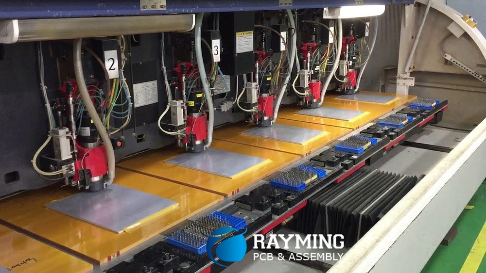
PCB Layout
- Capture schematics and create PCB newtork
- Route boards emphasizing signal, power integrity
- Iterate on physical design verifying performance
PCBs transform circuits into working prototypes.
Enclosure Integration
- Model mechanical enclosures with hardware
- Ensure components fit 3D envelopes
- Confirm production manufacturability
Unified electro-mechanical development enables robust products.
Firmware / Software
Well-architected firmware and software cement user experiences:
Platform Selection
- Evaluate middleware, operating systems, drivers
- Choose frameworks suiting architecture needs
- Enable rapid iteration on application code
This establishes a solid foundation.
Application Development
- Program feature-rich functionality
- Implement intuitive graphical interfaces
- Connect peripheral devices
- Validate functionality against requirements
Carefully coded firmware powers products.
Testing/Debugging
- Simulate hardware-software interactions
- Stress test limits of performance
- Identify memory leaks, race conditions, bottlenecks
- Enhance reliability prior to release
Comprehensive testing prevents field issues.
Cloud & Security

Connecting products to the cloud unlocks capabilities:
Cloud Integration
- Define remote services like storage,analytics
- Architect local-to-cloud data flows
- Manage user accounts/access
- Scale infrastructure with growth
Cloud abilities encourage innovation.
Data Protection
- Perform threat modeling to identify risks
- Apply latest encryption schemes
- Continually probe systems for vulnerabilities
- Isolate privileged functions and memory
Vigilance maintains trust.
Compliance Scope
- Assess regional device compliance needs
- Consult cybersecurity standards
- Implement mandated features accordingly
- Pursue certifications instilling confidence
These practices uphold security and safety.
Manufacturing
Successful manufacturing requires astute planning:
Process Selection
- Evaluate candidate build processes
- Request prototype quotations
- Assess technical ability, quality, lead times,location
- Qualify supply chain flow
This reduces downstream obstacles.
Design for Manufacturing
- Simplify mechanics, electronics, software
- Standardize components, processes
- Apply DFM principles boosting yield
- Collaborate with production engineers
Manufacturability cuts costs.
Quality Management
- Codify quality program procedures,audits
- Continually inspect, measure, test
- Manage non-conforming material
- Meet industry best practices
Excellent quality maintains reputation.
Branding & Marketing
Connecting with users drives adoption:
Brand Identity
- Define visual language, logo,styles
- Express brand values, personalities
- Apply across touchpoints consistently
This ignites emotional connection.
Content Creation
- Craft marketing materials, websites
- Engage audiences on social platforms
- Produce video demonstrations
- Inspires with storytelling
Compelling content grabs interest.
Market Launch
- Issue press releases for announcements
- Brief media outlets, bloggers
- Exhibit at key trade events, conferences
- Listen to user feedback post-release
Launch sets the tone for success.
Sales & Distribution
Hybrid sales strategies expand reach:
Direct Sales
- Enable online purchasing
- Offer free trials to spur adoption
- Provide sales engineering support
Channel Partners
- Recruit resellers, integrators
- Educate partners on solutions
- Incentivize channel activities
Retail Presence
- Land shelf space in stores
- Train in-store experts
- Supply marketing collateral
This sales mix hits more customers.
Post Purchase Experience
Customer experiences build loyalty:
Customer Support
- Staff help lines to promptly resolve issues
- Monitor social feeds for complaints
- Expedite replacing damaged units
Community Building
- Foster user forums, groups
- Encourage customers to submit ideas
- Celebrate brand advocates
Upgrade Path
- Notify customers of new features
- Offer discounted expansion modules
- Provide hassle-free installation
Positive engagement sparks referrals and repeats sales.
Conclusion
Creating breakthrough electronic products requires cross-discipline mastery spanning electrical, mechanical, software, cloud, business, and manufacturing realms. By applying user-centricity, sound engineering principles, methodical project execution, and commercial mindfulness, innovators can shepherdideas from concept to shipped product. This guide presented a holistic framework encompassing the entirety of successfully developing, producing, and supporting the next great electronic device. With vision, rigor, and passion, transformative products that people love stand ready to be brought to life.
Frequently Asked Questions
Q: What is most important for new product success?
A: Obsessively focusing on understanding real customer problems and designing elegant solutions tuned to user needs in a simple, intuitive way. Technology for technology's sake fails. Lead with the customer experience.
Q: What causes most new electronics startups to struggle?
A: Lack of business, marketing, and manufacturing planning beyond just the core product engineering. Building a company takes well-rounded teams, not just a novelty invention.
Q: Should you patent ideas early?
A: Potentially, but only for truly novel inventions. More important is maintaining confidentiality during development and being first to market with speed. Executing well outpaces idle patent portfolio.
Q: What electronics innovation areas are hottest right now?
A: Sustainability tech, IoT/edge devices, AI/computer vision hardware, augmented/virtual reality, quantum computing, flexible/wearable electronics, robotics, and precision healthcare electronics.
Q: How can makers ensure reliable offshore manufacturing?
A: Careful vetting, requirements reviews