Friday, January 26, 2024

What is 2+N+2 PCB Stackup Design for HDI Boards

 High density interconnect (HDI) printed circuit boards (PCBs) utilize tighter trace/space to enable higher component density and more routing channels. To facilitate routing dense designs while controlling costs, 2+N+2 stackups are often adopted using microvias to transition between layers.

This article provides guidelines on 2+N+2 HDI stackup design, examining layer configurations, material selections and key considerations for maximizing performance. Best practices for minimizing via stubs, maintaining impedance control and handling power delivery are also covered.

HDI Stackup Overview

A 2+N+2 stackup contains:

  • 2 outer signal layers
  • N number of internal signal layers
  • 2 “low loss” plane layers placed strategically within the stackup

This cost-optimized arrangement provides a balance of signal routing, shielding, power delivery and thermal conduction.

Layer Planning

Careful planning of the 2+N+2 layer stackup ensures all design requirements are adequately met.

Layer Count

The number of layers (N) is selected based on routing density needs and lane count requirements for high speed interfaces. Layer transitions through micro/blind vias minimizes via stub length.

Layer Order

Internal layer order has implications for shielding, power delivery and heat dissipation that must be considered. Tradeoffs are usually required.

Plane Layers

Strategic placement of the two plane layers helps control costs while providing power, shielding and mechanical stability where needed most.

Material Selection

HDI designs require specialized materials to enable fine features reliably while controlling costs.

Dielectrics

Low loss, tight tolerance dielectrics with Dk values under 3.5±0.1 allow microvia stacking while ensuring impedance control and signal integrity. Common options:

  • Polyimides (HT)
  • FR408HR
  • Isola 370HR

Copper

1⁄2 oz copper foil is standard for HDI layers to optimize line width/space while minimizing surface roughness. 1oz copper may be used for thicker outer layers requiring higher current.

Surface Finishes

ENIG or Immersion silver provide durability while minimizing thickness (2–4μm) for the fine pad/via structures used. These finishes also facilitate probe inspection.

[Table summarizing typical HDI board material selections]

Transmission Lines

Controlling matched impedance transmission lines enables multi-GHz signals on HDI designs.

Trace Geometry

With 1⁄2 oz copper, trace width and space of 3/3 mils is typical. This facilitates 50Ω lines using standard HDI dielectrics. Line width may taper when transitioning layers.

Differential Pairs

Length matching between pairs controls skew. Serpentine routing or meandering helps match physical length. Minimum bending radius rules apply.

Vias

Microvias (0.2mm diameter or under) allow dense via transitions between layers with minimal stubs. Laser drilled through hole vias are still used sparingly for connectivity to thicker multilayer portions.

[Figure showing example controlled impedance traces with length matching and microvia transitions]

Power Distribution

Distributing power across HDI designs brings challenges of high current density and minimizing plane splits.

Power Planes

The 2 “low loss” plane layers are typically used for power distribution to shield signals and serve as low impedance AC current returns. Power nets may still require supplementary polygons on signal layers.

Decoupling

Given narrow power layers, dense passive decoupling placements are needed adjacent to each IC to combat inductance and supply noise. Microvias connect surface caps down to the low loss plane layers.

Thermal Considerations

High power density requires careful thermal analysis with placement optimized to avoid hotspots. Careful component selection together with sufficient vias to inner plane layers also helps dissipate heat.

Design Guidelines and Rules

To aid reliable fabrication and assembly at acceptable yields, design guidelines and rules must be applied during layout.

Routing

  • Match line lengths and geometries for differential pairs
  • Adhere to microvia stub length maximums
  • Breakout blind/buried vias cleanly allowing for annular ring tolerances

Planes

  • Minimize plane layer splits
  • Thermally balance power dissipation
  • Include guest islands in planes for decoupling caps

Manufacturing

  • Apply fabrication shop DRC rules
  • Set adequate manufacturing tolerances
  • Accommodate via aspect ratio limits

Following these guidelines improves manufacturability while also enhancing electrical performance.

Conclusion

A 2+N+2 stackup using microvias and HDI design techniques allows complex, high density PCBs to be manufactured reliably. By adopting the material selections, planning principles and design guidelines covered in this article, engineers can fully utilize this stackup to balance functionality, performance and cost.

Careful layer stack planning together with controlled impedance lines, appropriate decoupling and thermal considerations enables the practical implementation of multi-gigabit systems. As data rates increase and packages shrink, 2+N+2 HDI PCBs will only become more widespread across electronics sectors.

Frequently Asked Questions

Why are low loss dielectrics important for HDI stackups?

Low loss dielectrics with tight dielectric constant (Dk) tolerances enable controlled impedance lines essential for multi-gigabit data lanes. Low loss also ensures signal integrity by minimizing attenuation at RF frequencies.

What considerations influence the selection of internal layer count?

Primary drivers for internal layer count selection include:

  • Routing density requirements — more lanes and tighter geometries need more layers
  • Achieving target component placement density and footprint efficiency
  • High speed interface lane count and routing
  • Overall board thickness / rigidity targets

How can I minimize reflection and insertion loss on HDI lines?

Reflections distort signals, cause EMI and increase insertion loss which degrades signal integrity. Controlling line impedance, minimizing discontinuities, length matching, proper termination schemes and using low-loss dielectrics all help reduce reflections and insertions loss.

Why does having a reference plane above and below each signal layer help?

Closely spaced reference planes on adjacent layers provide front-to-back shielding that contains electromagnetic (EM) fields within the dielectric. This prevents crosstalk coupling between traces while also allowing wider lines with better impedance control due to the stronger EM field containment.

What typical features indicate a PCB is manufactured with HDI technology?

Typical giveaways are trace/space ≤ 6 mil with microvias visible between layers under X-ray. HDI designs also often have higher component densities, fine precision manufacturing tolerances, laser via drilling and specialized materials used.

How to Work with IEEE Symbol Objects on a Schematic Library Sheet

 When creating schematic diagrams for electrical and electronic circuits, it is common to use standardized symbols from libraries such as those defined by the Institute of Electrical and Electronics Engineers (IEEE). Using these standardized symbols helps improve clarity and ensures that schematics are universally understood by engineers and technicians.

This article provides a step-by-step guide on how to work with IEEE symbol objects on a schematic library sheet within electrical CAD software. It covers the basics of inserting symbols, editing symbol properties, using parameters and meta-data, and optimizing symbols for reuse. Advanced topics such as scripting and creating custom shapes are also introduced.\Getting Started with the Schematic Library

Most Electrical CAD (ECAD) software used for printed circuit board (PCB) design will include a library of common IEEE symbols. However additional libraries can also be imported if required. When working with library symbols, there are a few key concepts to understand:

Schematic Library Structure

  • Symbol: The visual object placed on the schematic sheet. This contains the graphical shape(s).
  • Footprint: The physical footprint used on the PCB to represent the part. This is associated with the symbol.
  • Meta-data: Additional data such as description, keywords, manufacturer part numbers etc.

Inserting a Symbol

To insert a symbol from the library on to the schematic:

  1. Open the schematic library manager
  2. Browse to the symbol you wish to use
  3. Select the symbol and place it on the schematic sheet

[Table for Inserting an IEEE Symbol from the Library]

StepAction1Open schematic library manager2Browse to desired symbol3Select and place the symbol

Editing Symbol Properties

Once placed on the schematic, symbols can have their properties edited. This allows customization of each instance without altering the original library symbol.

Editing Graphical Properties

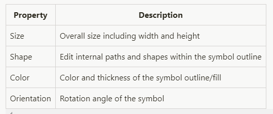
Graphical properties such as size, shape, color and orientation can be edited per symbol. This allows symbols to be tweaked to suit the specific schematic layout requirements without changing all instances globally.

To edit graphical properties:

  1. Select the symbol instance(s) to edit
  2. Open the properties dialog
  3. Edit properties like size, shape, orientation as needed
  4. Save properties to apply changes

[Table for Editing Graphical Properties of a Symbol]

Editing Meta-data Properties

Non-graphical properties like the description, footprint association, manufacturer part number and keywords can also be edited per symbol instance:

To edit meta-data properties:

  1. Select the symbol instance(s) to edit
  2. Open the properties dialog
  3. Edit text metadata like description, keywords etc.
  4. Save properties to apply changes

This meta-data is used when generating reports (BOMs, parts lists etc) and can improve clarity of the design intent.

[Table for Editing Meta-data Properties of a Symbol]

Using Parameters

Parameters are special metadata properties that allow instances of a symbol to be configured without editing the library symbol itself. They create variations of a symbol dynamically.

Common examples include:

  • Configurable power symbols showing voltage, current etc.
  • Component symbols with variable number of pins
  • Symbols representing different physical sizes, shapes and configurations

To use parameters:

  1. Ensure the library symbol has parameters defined
  2. When inserting the symbol, edit parameters as needed
  3. Parameters can be changed later by editing properties

Parameters use special syntax, for example {NAME} refers to the parameter called "NAME". When edited, this syntax is replaced with the desired value.

[Table for Using Parameters on an IEEE Symbol]

Using parameters helps reduce library bloat by avoiding near-identical copies of symbols. They also improve efficiency when designing variants of circuits or components.

Scripting and Customization

For advanced users who want maximum control and customization ability, symbols and entire libraries can be created or edited through scripting and programming.

While graphical editors provide an intuitive way to edit symbols visually, scripting allows bulk changes to be applied across entire libraries easily.

Symbol Scripting

Symbol shapes can be described using code rather than interactive graphical editors. For example:

RECTANGLE(-100,-50)(100,50)  
CIRCLE(0,0,30)
TEXT(0,70,'Place text here',10)

Scripting provides fine-grained control over shapes and position while also enabling automation through code.

Library Scripting

Entire schematic symbol libraries can also be generated using scripts. This allows custom libraries tailored to specific requirements to be created programmatically.

For example, the following script creates a simple library with a single symbol:

NewLibrary(MyCustomLibrary)
NewSymbol(Symbol1)
AddRectangle(...)
AddCircle(...)
EndSymbol
EndLibrary

This improves efficiency when dealing with large libraries or specialized symbol sets. Scripted libraries can also integrate directly with other electronic design automation workflows.

Creating Custom Shapes

For one-off symbols that use completely custom graphical shapes, the underlying CAD tool’s shape editing features can be used. This allows users to design shapes perfectly suited to application-specific symbols.

Advanced tools even allow import of graphics from external vector drawing tools. This provides maximum flexibility when dealing with unusual or highly specialized symbols.

Optimizing Symbols for Reuse

When creating schematic libraries, making symbols reusable across projects improves efficiency. Here are some tips:

  • Use parameters so symbols can adapt without editing
  • Include comprehensive meta-data like descriptions, keywords etc.
  • Modular design allowing common sections to be reused
  • Consistent graphical style aids recognition
  • Script libraries to allow automation where possible

Applying these principles helps transform a basic set of schematic symbols into a professional, reusable library resource.

Integrating Symbols into the Wider Design Workflow

To fully realize the benefits from IEEE standardized schematic symbols, it helps to integrate their use into the wider electronics development process spanning schematics, PCB layout, manufacturing and beyond.

Schematic-PCB Integration

Linking schematic symbols to matching PCB footprints ensures accuracy is maintained across both design files. Any change to one is automatically reflected in the other.

BOM and Reporting

Including comprehensive meta-data in all library symbols improves downstream BOM generation and reporting clarity. Standardized fields like manufacturer and part number integrate with procurement and manufacturing processes smoothly.

Design Reuse

Using modular symbols based around reusable sections helps improve design efficiency across projects. Adopting common graphical styles also aids recognition when revisiting previous designs.

By considering the entire electronic product development workflow, efficiency gains from standardized symbol libraries are multiplied while also reducing errors.

Frequently Asked Questions

How do I add new symbols to my existing library?

Opening the schematic library editor allows new symbols to be added to existing libraries the same as when creating a new library. Ensure any new symbols follow consistent graphical styles and meta-data formats for clarity. Scripting libraries also makes it easy to append additional symbols.

My symbols display incorrectly scaled on the schematic sheet. How do I fix this?

Check whether the symbol has a defined “real world” size set in its properties. If so, disable auto-scaling or manually set the instance’s size as needed. Changing units settings of either the library or schematic can also help resolve scaling issues.

I have an unusual custom symbol requirement. What is the best way to handle this?

For one-off specialist symbols, using the inbuilt CAD drawing tools to create custom shapes is the most flexible approach. Importing SVG graphics or utilizing symbol scripting are also options. For maximum reuse, isolate any common or generic graphical portions into separate base symbols where possible.

How should I name symbols and metadata fields consistently?

Adopting an internally consistent naming convention helps minimize confusion. For example, descriptive names for symbols themselves, consistent units/terms, and standardized field labels for properties improves clarity

Popular Post

Why customers prefer RayMing's PCB assembly service?

If you are looking for dedicated  PCB assembly  and prototyping services, consider the expertise and professionalism of high-end technician...